
At the beginning of the development of a System-on-Chip, typically the RTL (register-transfer level: an abstract level used to describe the operation of digital circuits usually written in VHDL or System Verilog language) is written to meet a set of requirements which can be internally (organisation creating the solution) or externally (customer) generated. In order to determine whether those requirements have been met i.e. the design is correct, a number of different verification tasks (read more about verification) are performed. An example of one of these tasks is functional simulation, in which the functions described within the RTL code are simulated within a controlled software environment.
However, there are aspects of the design which cannot be easily verified (if at all) using functional, or even physical, simulation. For example, testing communication interfaces which are connected to off-chip components or running software on the hardware design cannot be performed accurately or efficiently within a software environment.
Prototyping tests the chip as a whole
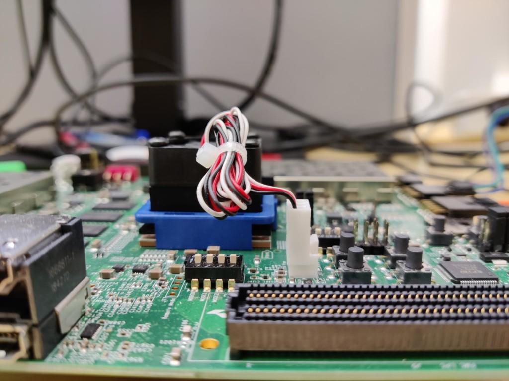
Prototyping is a process that is executed in addition to the verification of the chip. In prototyping, the RTL (register-transfer level) description of the chip is synthesized to the programmable chip, which then works in a similar way to the final chip. This can be done with an FPGA development kit. It provides a physical platform which can run hardware designs significantly faster than the software simulations and can perform a level of verification which would not be feasible in software.
FPGA synthesis takes several hours but it needs to be done only once, and after that, the chip can be booted. The main difference between the FPGA prototype and the actual chip is the performance: if the clock speed of the chip would be 1 GHz then the FPGA execution could reach 100 MHz.
Tom Szymkowiak from Tampere University does FPGA prototyping in the SoC Hub team. He explains what his work means in the context of SoC Hub:
“Whilst it is possible to run hardware designs at a high level of fidelity using FPGAs, it should be noted that due to the architecture of an FPGA, some aspects of a complex SoC/ASIC design (such as SoC Hub’s Ballast) must be modified in order for it to be run. Therefore, my key tasks are related to gaining an understanding of how each subsystem of the SoC is designed and implemented and determining how best to implement them onto an FPGA in a way that it accurately represents the original design but can also be run and tested on the platform with ease.”

A key aspect of the prototyping is that it cannot be started effectively until there is a level of confidence in the operation of the design which is gained through simulation.
“Once we were at that point, there was a period of mobilisation, in which we determined exactly what the scope of the prototyping would be and what tools would be appropriate. Once we had agreed on a path to take, we started the effort to prototype some of the key aspects of the SoC,” Tom says. For example, a major aspect of the SoC operation (which is difficult to test in simulation) is the boot process of the chip. Therefore, a concerted effort was made to complete the prototyping of the subsystem responsible for this functionality as soon as possible to help ensure that the ASIC will initialise correctly.
“We achieved this goal and it highlighted some issues which would in all likelihood not have been identified prior to tape-out if the prototyping had not been completed. It was great to witness the boot operation successfully running on the FPGA,” Tom continues.
What happens next?
Prototyping benefits the software developers too: the prototype works like the actual chip and it can be used as a software development platform. This is the next phase in the FPGA prototyping now that SoC Hub’s first SoC Ballast has been taped out.
“At the moment we are focused on prototyping the high-performance subsystems to provide the software team a platform which they can use to accurately develop the software which forms the board support package for the chip. We are also preparing for the next iteration of the chip,” Tom says.
Working in SoC Hub has complemented Thomas’ studies and given him the opportunity to put his skills to test in practice. Even though FPGA tools may have a reputation for being a bit tricky, he says that the experience of working for the project has been fantastic.
“Since starting my MSc last year, my interest in hardware and low-level software development has grown exponentially. Joining the project and working on the FPGA prototyping has provided me with a great amount of exposure to both of those. It is essential that you have a good knowledge of both the hardware and software when trying to prototype an ASIC using an FPGA. With the support and knowledge of the SoC Hub team as well as the cutting-edge resources provided by Tampere University, it has been a very enjoyable and enrichening experience so far,” Tom concludes.
