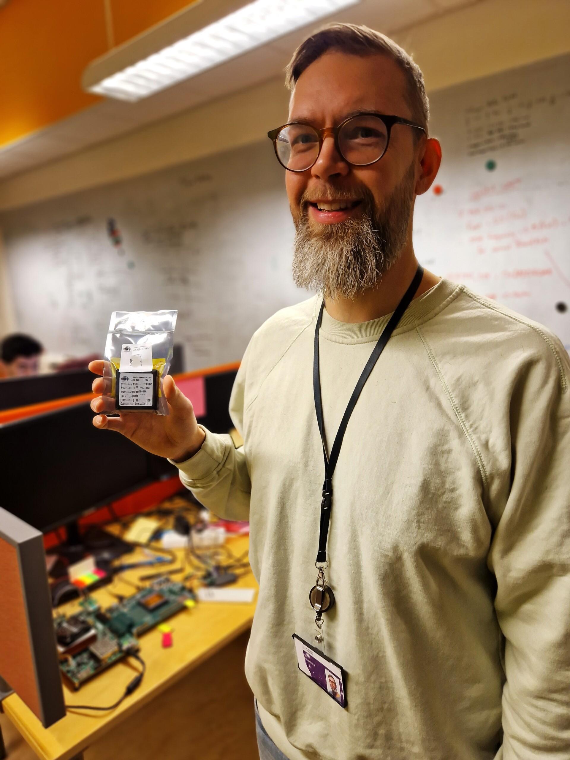
Three System-on-Chips taped out in three years – that was the main objective of the first project of SoC Hub, bringing academia and industry together to collaborate. Agile practices were applied to reach this goal, with selected key principles forming the project’s framework. How was this ambitious SoC development goal achieved? This question is explored in an article that assesses the project. The article’s author and project manager, Antti Rautakoura from Tampere University, summarizes the key findings.
Preparing for the project began in 2018. At that time, Tampere University recognized the need to boost SoC development expertise in Finland and started making action plans with the project’s main partner, Nokia.
Setting up the virtual organization for the project consortium started in 2020. COVID-19 pandemic had just hit the world, so the SoC Hub consortium had to work mainly as a virtual team. The work started from scratch, building a collaboration platform with EDA tools and technology libraries, as well as making necessary agreements. After this, the actual SoC design work could begin.
“Our main objective was to tape out one SoC every year, and the work was scheduled according to this principle. We wanted to maintain the yearly tape-out cadence since the leading idea was to do fast-paced hardware development,” says Antti Rautakoura who acted as a project manager for the SoC Hub project.
Diverse teams and low hierarchy

The work was done in diverse teams. Some tasks were dedicated to individual experts with longer
experience but mainly the project was built on small sub-system teams of 2–4 persons. The project members had varying experience levels, ranging from beginners to senior-level experts. More experienced team members acted as mentors for junior professionals.
“In many cases, the same developer participated in multiple different design activities, which does not typically happen in the industry. We had very low hierarchy in our organization, which turned out well. Scaling this to the industry may have its challenges but companies should consider a similar model in their work,” suggests Rautakoura.
SoC Hub taped out three System-on-Chips that are regarded as a set. The chips were Ballast (15 mm2), Tackle (4 mm2) and Headsail (25 mm2). They consisted of several subsystems, with physical design was done in parallel, which accelerated design turnaround time. Open-source IPs were used, but there was also in-house IP development to extend the portfolio. The expertise and challenge level increased during the project, and by the end of 2023, the team was able to develop a 300-millon transistor SoC in a year.
Feedback from the full design cycle ensures successful completion
Development of complex SoCs requires multiple iterations. Rautakoura describes the benefits of this approach:
“One of the key advantages is that the project receives feedback from the full design cycle. Although this might sometimes result in not meeting all requirements for the current iteration, early feedback ultimately accelerates the design’s completion.”
Some challenges were faced along the way, but the one-year tape-out cadence was maintained.
“We considered a predictable schedule and fixed cadence to be important principles in agile development. The IP selection, development and integration should align with the planned tape-out schedule,” says Rautakoura.
What were some valuable lessons learned during the project?
“First, we learned that making contracts with the technology providers takes 3-6 months, so that time needs to be reserved at the very beginning. However, this affected only the schedule of the first chip since this effort didn’t have to be repeated. Second, IC package and PCB design must be started at the same time as the architectural planning,” Rautakoura says.
SoC Hub demonstrated that a hundred-million transistor SoC can be taped out in a year with a team of 20 people. This experience led to the creation of a platform for continuous development. The project also established a long-lasting legacy with a framework for collaboration in multi-partner projects and a template for future SoC designs.
Read the full article in IEEE Micro

