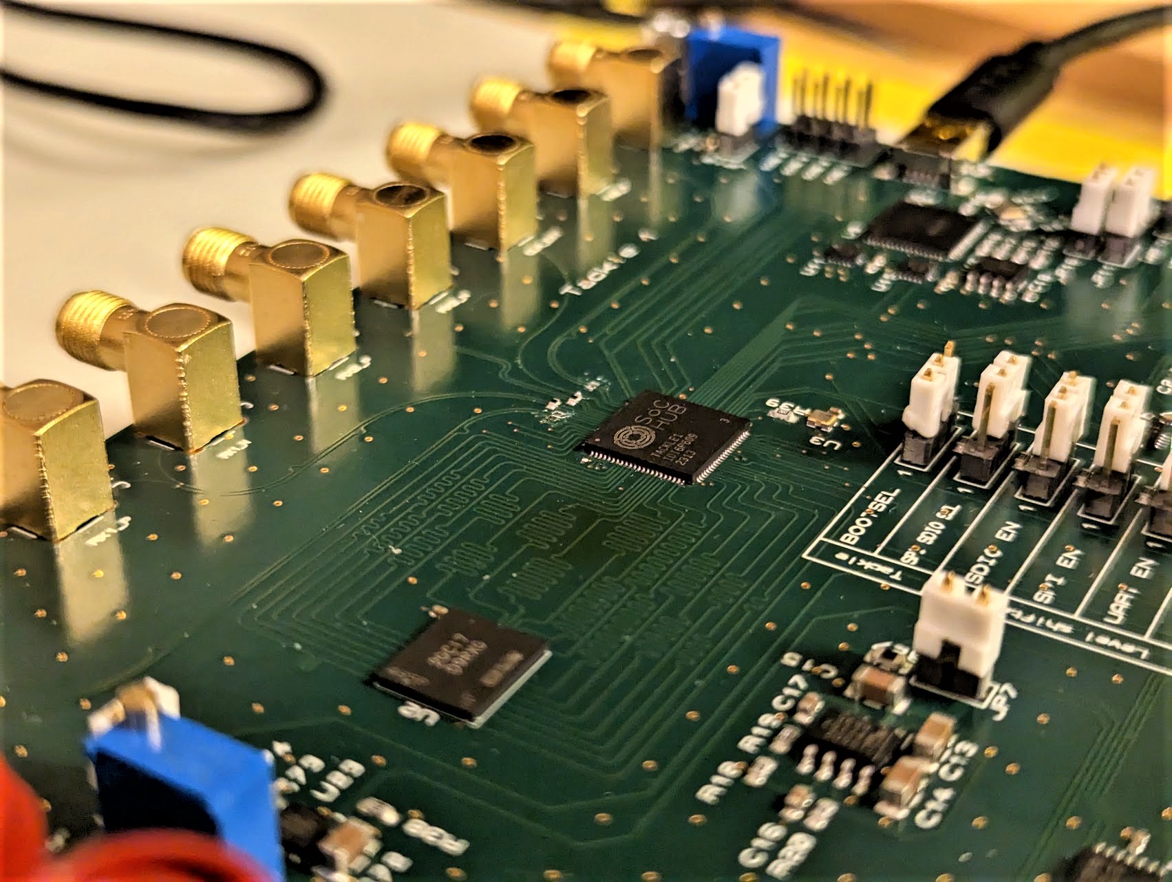
The second SoC Hub chip Tackle was taped out in November 2022 and sent to manufacturing to TSMC. The chip samples arrived from packaging to Tampere University in April, and the team started to wake up the chip right away. Wake-up, which is the first testing task, shows whether the design of the chip has been successful.
– The testing of the chips started with electrical checking. The electronics lab staff ensured that the Tackle chip was soldered correctly on the PCB, and the power rails and clock signals were correct. After these checks, the chip and the PCB were declared ready for waking up, says Arto Oinonen who leads the testing process at Tampere University.
The experiences of the previous Ballast chip and FPGA prototyping work allowed a rapid start for the wake-up process. The tools and the environment were already set up, and the process was familiar for the team. Already during the first wake-up day the team found out that the CPU core can access all the subsystem register domains, clock generating PLLs work, and both the onboard SRAM and external SDRAM memories can be accessed.
– It is always exciting to power up a chip for the first time. It is not certain the chip functions at all, but seeing the first response from the CPU to JTAG is a great success. It is also not uncommon to see errors at first, but finding the root cause for those is part of the wake-up process. For example, the SDRAM memories have complex timing parameters, and it is normal to see some data bits flip from 0 to 1 before the timing is fine-tuned for the specific memory part, describes Oinonen.
The next focus is on waking up the Serdes TX/RX link. After that, the testing continues to higher level software tests and performance measurements. All the base requirements for code execution have been checked: in addition to the memories, also the CPU interrupts, the UART serial port and DMA controller work correctly.
The Tackle die area is 4 mm2 and it was fabricated on TSMC 22nm Ultra-Low Leakage technology and assembled to 88 pin QFN IC package. The developed new IPs are essential in reaching the project’s targets for the third chip Headsail focusing on high-performance computing on low-power technologies.
In fact, Tackle consists of two different chip variants produced in the same tape-out: Tackle1 and Tackle2. Both variants include a small Ibex RISC-V core, a programmable DMA controller IP, a high speed Serdes datalink, and an SDRAM memory controller. The difference between the variants is that the Tackle1 memory controller is configured for LPDDR1 while the Tackle2 has support for LPDDR2 memory.
All together SoC Hub consortium will design three chips in the project funded by Business Finland. The project partners include Tampere University, Nokia, CoreHW, VLSI Solution, TTTEch Flexibilis, Procemex, Wapice and Cargotec.
Before the Tackle chip, the first SoC Hub chip Ballast was taped out late 2021 and after receiving the chips in June 2022, a successful chip wake-up testing was carried out. Following agile project practices, the development of Tackle started already in parallel with the development of Ballast. The third chip named Headsail will be taped out mid-2023.
